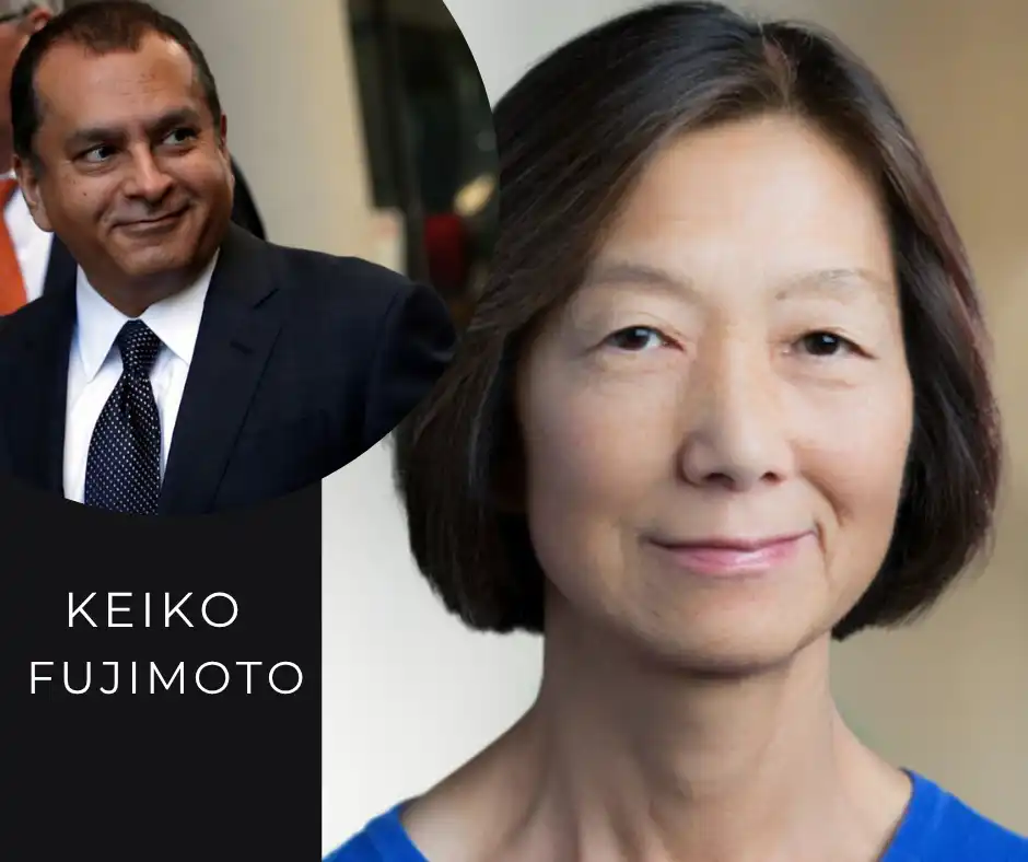
In official documents, Keiko Fujimoto is known as the former wife of Ramesh (Sunny) Balwani, who was the former Theranos president, but her life story is that of a long and disciplined technical communication, design, and artistic professional career that grew apart from that relationship. Trained in Japan and the United States, she worked over thirty years in the semiconductor industry, especially at Applied Materials, where she provided technical documentation and publications management while maintaining a sense of connection to Japanese aesthetic traditions. Her narrative shows how a personal career life may be based on craftsmanship, cultural identity, and accuracy even in situations when the mass media focuses on it.
Summary of Keiko Fujimoto
| Detail | Information |
| Last Name | Keiko Fujimoto |
| Date of Birth | Privately held |
| Place of Birth | Japan |
| Nationality | Japanese |
| Ethnicity | Asian |
| Education | B.A. in International & Cultural Studies, Tsuda University; M.S. in Information Sciences, University of Illinois Urbana-Champaign |
| Profession | Artist, Designer, Technical Publications Manager |
| Famous For | Applied Materials career and previous marriage to Sunny Balwani |
| Career Duration | 1988 – 2021 |
| Major Role | Technical Publications Manager, Applied Materials |
| Television Appearance | Takajin Mune Ippai (Japan) |
| Marital Status | Divorced |
| Ex-Husband | Ramesh Sunny Balwani |
| Languages | Japanese and English |
| Estimated Net Worth | Approx. 150,000 (public estimate) |
| Present Condition | Retired, indulging in art and personal life |
| Residence | Japan (reported) |
Childhood and Cultural History
Keiko Fujimoto was born and grew up in Japan, where artistic feeling and technical discipline tend to grow hand in hand. The Japanese cultural tradition supports simplicity, balance, and attention to detail both in everyday life and in professional activity. These principles formed her perspective at a young age and subsequently informed her writing on technical matters and art design.
She adopted ideas like wabi-sabi, which considers imperfection as beautiful, and ma, which attaches importance to meaningful space and balance, in both her creative and professional philosophy. Instead of seeking popularity, she developed a quiet and systematic way of working that focused on clarity and usefulness. This cultural underpinning was evident in her career, especially in the manner in which she structured information and her visual design.
Her initial background promoted discipline and patience, which would be critical in technical documentation and administration in intricate engineering sectors in the future.
Academic Development and Education
The academic career of Keiko Fujimoto can be characterized as having both cultural and technical interests. She pursued International and Cultural Studies at Tsuda University in Japan, where she acquired a broad perspective on international communication, language, and cross-cultural interaction. Such an educational background equipped her to operate in cross-cultural settings and interact effectively with people from different backgrounds.
She went on to obtain a Master of Science in Information Sciences at the University of Illinois Urbana-Champaign in the United States. This higher qualification enhanced her critical and technical abilities, especially in the structuring and delivery of intricate information. Information science is concerned with organizing knowledge in a manner that makes it easily available and practical, which is similar to technical documentation and engineering communication.
This combination of liberal arts study and technical preparation gave her a unique edge. She could comprehend not only human communication but also technical systems, allowing her to translate complicated engineering processes into coherent and trustworthy documentation.
Initial Work Experience in the Semiconductor Industry
Keiko Fujimoto started her career in the late 1980s in the semiconductor industry, where documentation must be accurate and safety and engineering standards must be observed precisely. The role of technical writers in this industry is to produce manuals, operational guides, and process documentation that assist engineers and technicians in using sophisticated equipment safely and efficiently.
At the beginning of her career, she was employed in the production of technical manuals, installation guides, and operating manuals. These documents had to be precise, consistent, and coordinated with engineering teams. Semiconductor equipment is very intricate, and any slight documentation error could cause both operational and financial losses. Technical communication is therefore paramount in ensuring product reliability and safety.
It was during this time that she developed technical editing skills, knowledge organization skills, and engineering communication skills. Her ability to collaborate closely with engineers and translate complicated information into easy-to-follow instructions contributed to her gaining the status of a trusted professional.
The Applied Materials Leadership
Keiko Fujimoto has approximately thirty years of work experience at Applied Materials, one of the leading manufacturers of semiconductor equipment. She later became Technical Publications Manager, a post in which she led, planned, and coordinated with other departments over time.
As a manager, she had the responsibility of:
- Supervising documentation teams
• Developing editorial standards
• Developing templates and manuals
• Working in collaboration with engineering and product teams
• Ensuring consistency in worldwide technical publications
• Managing international market localization
Her work contributed to standardizing technical documentation processes and enhancing communication between engineers, field service teams, and customers. Clear documentation minimized errors, decreased training duration, and enhanced product usability, making it an indispensable component of industrial operations.
Her leadership was based on clarity, accuracy, and user-focused communication. She did not consider manuals as secondary materials but regarded them as tools that facilitate technology and ensure safe operation.
Also Read: Keelin Noel Garcia
Innovative Labor in Art and Design
Alongside her technical work, Keiko Fujimoto developed a keen interest in art and design. The same principles observed in her professional life—simplicity, balance, and thoughtful structure—were reflected in her artistic work.
Her creative expression incorporated Japanese aesthetics. Her artistic work was characterized by minimalist design, thoughtful use of space, and visual harmony. These aspects bridged her professional and artistic activities, showing that technical accuracy and artistic delicacy can coexist.
She also appeared in Japanese television shows such as Takajin Mune Ippai, which introduced her work and ideas to a broader audience. This exposure was limited, as she preferred to remain private. Her artistic contributions emphasize the significance of cultural identity in professional and creative performance.
Personal Life and Marriage with Sunny Balwani
The name Keiko Fujimoto frequently appears in the news due to her previous marriage to Ramesh Balwani, also known as Sunny. The couple lived in San Francisco at the beginning of his technology career.
Their marriage ended in 2002, a few years before Balwani joined Theranos. This timeline is significant as it indicates that Fujimoto was not involved in the company or its operations.
Following the divorce, she led a private life and did not comment publicly on the subsequent legal issues of her former husband. This choice demonstrates her preference for privacy and professional autonomy. Her identity and career developed independently of the circumstances that eventually brought Balwani into the media spotlight.

Theranos Background and Media Focus
Keiko Fujimoto’s name is well known to many readers investigating the Theranos scandal. Theranos became one of the most discussed business frauds in recent history. The company claimed to pioneer blood-testing technology but ultimately faced lawsuits and criminal charges against its executives.
Sunny Balwani, president and chief operating officer, was a key figure in the case. Public interest in his personal life led to searches for individuals associated with him, including Keiko Fujimoto.
However, her marriage to Balwani ended years before Theranos was founded. She did not participate in the company’s operations, legal matters, or corporate activities. Her relationship is historical, not professional or legal. This distinction is critical in understanding her biography.
Also Read: Karen Weitzul
Life Post-Divorce and Return to Japan
After her separation from Sunny Balwani, Keiko Fujimoto reportedly spent more time in Japan and focused on her professional and artistic work. This period marked a return to cultural roots and an increased emphasis on personal privacy.
Rather than engaging with media attention, she concentrated on her career and creative interests. This approach allowed her to maintain independence and avoid unwarranted public exposure.
Her post-divorce life reflects resilience and autonomy, demonstrating how individuals can continue building meaningful careers while remaining outside the media spotlight.
Retirement and Present Life
After more than three decades in the semiconductor industry, Keiko Fujimoto retired around 2021. Retirement allowed her to step away from corporate responsibilities and concentrate on personal interests, especially art and culture.
Her professional legacy continues through the documentation systems, editorial standards, and teams she helped develop. Technical publications produced under her leadership remain valuable to engineers and industry professionals.
She is believed to live a quiet and private life today, focusing on personal projects and creative endeavors. Her choice to remain out of the public eye reflects her long-standing preference for privacy and independence.
Career Lessons of Keiko Fujimoto
Several practical lessons can be drawn from her professional career:
- Technical communication is a vital aspect of engineering and industrial operations. Documentation enhances safety and efficiency.
- Cultural identity can strengthen professional practice. Japanese aesthetic principles influenced her clarity and structure.
- Long-term consistency creates a sustainable professional legacy. Over thirty years of dedicated work left a lasting impact.
- Privacy can be an intentional and effective personal strategy.
- Technical leadership often involves creating systems that support future generations of professionals.
Conclusion
The life of Keiko Fujimoto represents a diligent and mindful career grounded in technical accuracy, cultural sensitivity, and personal discretion. Despite being linked publicly to Sunny Balwani and the Theranos saga, her own achievements in technical publications and design are substantial. Over a lifetime in the semiconductor sector, combined with continued commitment to art and cultural values, she has created a quiet but purposeful legacy that demonstrates professionalism, resilience, and focus.
External associations should not overshadow her biography. Readers seeking to understand her life should focus on her education, long service at Applied Materials, artistic endeavors, and commitment to privacy. Her experience provides a model of how gradual work and cultural grounding can shape a lasting professional identity.
Frequently Asked Questions
- Who is Keiko Fujimoto?
Keiko Fujimoto is a Japanese technical publications manager, artist, and designer who had a long-term tenure at Applied Materials and was previously married to Sunny Balwani. - What is the education of Keiko Fujimoto?
She attended Tsuda University in Japan, earning a degree in International and Cultural Studies, and received a Master’s degree in Information Sciences from the University of Illinois Urbana-Champaign. - What is the relationship between Keiko Fujimoto and Theranos?
Before the company was founded, she was married to Sunny Balwani, a Theranos executive, but they divorced in 2002. She had no involvement in Theranos. - What did Keiko Fujimoto do at Applied Materials?
She was Technical Publications Manager, overseeing documentation teams and providing clear technical communication for semiconductor products. - Does Keiko Fujimoto work?
She retired in 2021 and is believed to be focusing on art and personal life. - What is the current residence of Keiko Fujimoto?
She is reported to live in Japan, maintaining a low-profile, private life. - What is the professional background of Keiko Fujimoto?
She has extensive experience in technical documentation, leadership in semiconductor publishing, and the integration of Japanese aesthetic principles with design and communication.